Capacitive Recursive DAC

The capacitive recursive DAC is mostly used in algorithmic ADCs. Rather than implementing all bit weights simultaneously with separate components, it works iteratively: each step adds the current bit’s contribution, scaled by
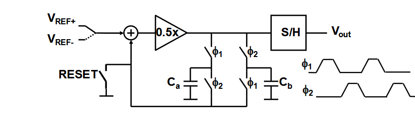
 , to the previously accumulated value.

LSB-first (gain )

Starting from the least significant bit, the recursive accumulation is:

Bit weights therefore run from at the MSB down to at the LSB.

MSB-first (gain )

The same structure applies when the gain factor is replaced by instead of :

Which approach is better?

Designing for a gain of requires an amplifier with only gain, which has a relatively relaxed dynamic range requirement. The MSB-first approach, by contrast, multiplies by at every step, which means any error in grows by by the time the LSB is reached, demanding a far more stable power supply. In the gain-2 implementation, internal node amplitudes and accumulated errors can grow exponentially through the recursion, making amplifier linearity and reference stability more demanding, but the LSB-first approach is preferred in practice because the amplifier constraints are much easier to meet.


Capacitive DAC

Capacitors are the most precisely matched components available in CMOS processes, which makes them a natural fit for DAC implementations. Resistive approaches such as R-2R ladders are less suitable here because large parasitic capacitances distort the intended resistor ratios, a bridge capacitor can be used as a workaround, but it adds complexity.

Capacitive DACs can be realised at low power since there is no static current path, but they do require some form of output buffer to drive a load.


D/A Converter Types

Among DAC architectures, current-steering is the fastest, capable of reaching conversion rates of around . The capacitive DAC sits between the voltage and current domains. The sigma-delta modulator takes a different approach: the output is a high-frequency pulse stream whose average value represents the desired analog level, when the pulse is high, it contributes ; the average over time gives the output.

A practical challenge with pulse-based outputs is that sharp edges are needed when two pulses appear close together, otherwise they blur into one another. The return-to-zero (RTZ) DAC addresses this by ensuring that after every bit’s on-time pulse, the output explicitly returns to zero before the next pulse begins. This guarantees a clean transition regardless of the bit pattern.

Sigma-delta feedback: why 1-bit?

In a sigma-delta modulator the feedback DAC is preferred to be 1-bit. The reason is linearity: a 1-bit DAC has only two output levels, and , and any two points define a perfectly straight line, the transfer characteristic is therefore inherently linear by construction. An -bit DAC has intermediate levels, each set by component matching; imperfections in that matching mean the transfer characteristic is no longer a straight line, introducing nonlinearity directly into the feedback path.


ADC Accuracy

The accuracy of an ADC is fundamentally tied to the ratio

For the analog steps to be equally spaced, the components that set those levels must be equal, matching quality directly determines linearity. Accuracy is limited at several levels simultaneously: batch-to-batch variation, wafer-to-wafer variation, and component-to-component variation within a single die.

Physical origin: doping fluctuations

In a CMOS process, the properties of a transistor are set by the doping atoms present in a given volume. A typical device might contain on the order of doping atoms. Because the number of atoms in any small volume is not a fixed quantity, different instances of nominally identical devices will contain slightly different numbers, there is an unavoidable physical source of mismatch.

Two regimes of variation are important to distinguish. Global variation shifts both devices in the same direction, so the effect largely cancels when the two are compared. Local variation shifts each device independently, producing a genuine imbalance between them.

Mismatch model

The total average dopant dose controls the average number of dopants in a given volume. The number of dopant ions actually present in any particular device follows a Poisson distribution with mean . For large this converges to a Gaussian distribution, and the key property is:

Area and matching

From the mismatch model (slide 93), the threshold voltage mismatch between two transistors follows:

where is a process-dependent mismatch coefficient. This relationship holds for MOS transistors and generalises to most matched component pairs. The implication is straightforward: larger area gives better matching, because a larger device averages over more doping atoms, reducing the relative fluctuation.

The mismatch coefficient is on the order of % per per . Physically, better matching corresponds to confining more field lines within a given area, the more tightly the device’s electric field is controlled geometrically, the less sensitive it is to local doping fluctuations. The trade-off is that a larger area also means a larger capacitive load and therefore higher power consumption.