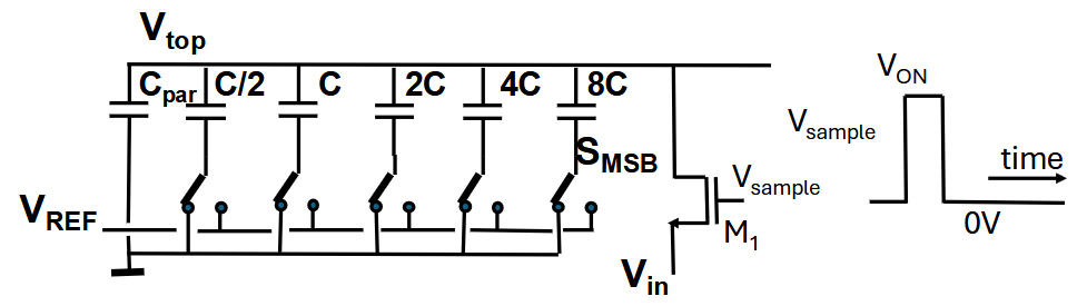
This capacitor array is often used in ADCs and DACs and is used for building a signal on
The voltage
Capacitor values:
etc.
Initially:
Input signal:
with
The sampling switch is implemented by NMOS transistor
Threshold voltage:
Current factor for a square transistor
Dimensions:
Oxide capacitance density:
Gate-drain overlap capacitance:
Use the strong-inversion square-law transistor equation.
Questions
A
Calculate the SNR after sampling.
To calculate the SNR we use the SNR formula
The total capacitance then is
So the SNR in dB is
B
The
How does the SNR change?
Since the two series capacitors will equal the single capacitor value, according to
However, there might still be slight parasitic effects that can cause some distortion.
C
After sampling, all switches are toggled to
What is the SNR?
Since the thermal noise was calculated during the sampling phase, in the conversion the switching to
D
A parasitic capacitance
is present from now on.
What is the SNR?
I assume this could make the SNR better, but will cause issues in concerns like matching and settling speed since it is capacitance introduced not by design. My motivation for the SNR going down comes from the earlier seen
So
E
Due to a design error, the bottom-plate-to-ground switch of
What is the SNR after sampling?
What is the SNR when, after sampling without ground connection of
Assume the
This means that the
so our new SNR is
→ What happens after connected to VREF? Doesnt matter only for when sampling.
F
The sample switch is implemented with an NMOS transistor
What is the minimum voltage for
Vt = 0.2 so VGS = 0.4 Since Vs is Vin, highest Vin is 0.3 + VDC
G
What is in that case the pedestal step?
Make a drawing of
VON and Vin ⇒ channel charge half charge to C (assumption)
delta V on C dg ⇒ 3 fC. Qgate is -(VGate) amplification 1.02x
H
What is the settling time for:
- the lowest signal level?
- the highest signal level?
use R ON and fast is 20ps low is 100ps, RON,low * Chold for slow
I
Sketch the expected distortion (THD) from DC to maximum frequency.
- HD2 - omega deltaRC / 4
J
Comparing the SNR and the THD, advise whether to:
- increase
- or decrease