Chapter 2.2 talks about the I/V Characteristics of the MOSFET. This will help us analyze the generation and transport of charge and will help us elevate our abstraction from device physics to circuit level.
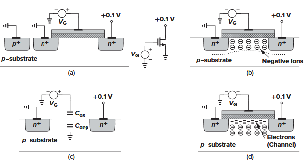
The gate, dielectric, and substrate form a capacitor, so as becomes more positive, the holes in the p-substrate are repelled from the gate area, leaving behind negative ions that mirror the charge on the gate. This is the creation of a depletion region.
As we increase , the width of the depletion region increases and the potential at the oxide-silicone interface also increases. This structure resembled a voltage divider consisting of two capacitors in series, the gate-oxide and the depletion region capacitor.
At a sufficient value a channel of charge carriers is formed under the gate oxide between S and D, the channel is inverted. The sufficient value is the threshold voltage .
is usually the gate voltage for which the interface is as much n-type as the substrate is p-type (for NMOS).
is the difference between the work functions of the polysilicon gate and the silicone substrate
is with the doping intensity and the density of the electrons in undoped silicon.
is the charge in the depletion region
is the gate-oxide capacitance per unit area.
The charge for if is the charge density in coulombs per meter and is the velocity of charge in meters per second gives
For we have that the charge placed on the gate must be mirrored at the channel.
The local difference at and depends on the position in the channel. is the full length of the channel, thus we subtract , or the voltage at the position, to calculate the charge density. This gives us
Now we substitute this into the equation for , and then integrate both sides, fill in , etc. to get