As a perquisite for the AD Converters course, it was recommended to me, due to my background in Computer Science, to study Design of Analog CMOS IC by professor Behzad Razavi during the course. I will not focus too much on solving the problems in the book since I already got enough to study, but will be using the book to gain more familiarity with the EE-topics needed during AD Converters. These notes will be raw, straight from the heart and may seem a bit rough.
MOS device basic physics
When operating as a switch, the transistor “connects” the source and drain together if 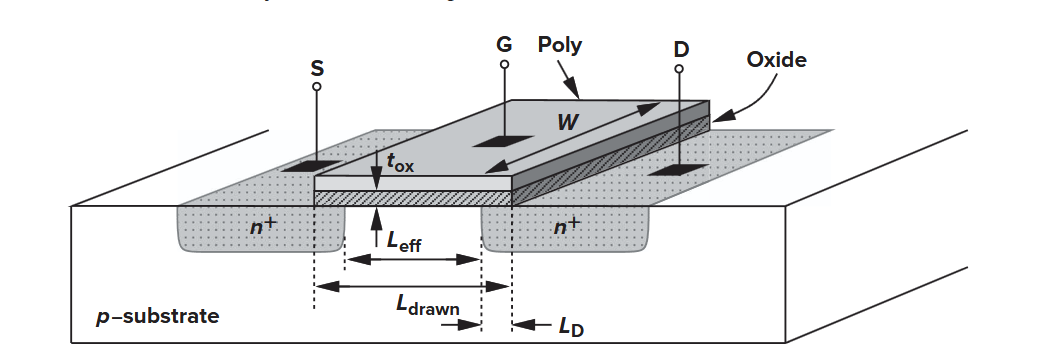 The image above shows a simplified structure of an n-type (NMOS) device fabricated on a p-type substrate. The device consists of two heavily n-doped regions forming the source and drain terminal, a heavily-doped and conductive piece of polysilicon operating as the gate and a thin layer of silicon dioxide insulating the gate from the substrate.
We call the dimension of the gate along the source-drain path length
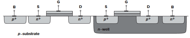
Typically the substrate is connected to the lowest supply in the system for an NMOS. N-well is connected to the most positive supply in the system. In a CMOS both NMOS and PMOS are used. PMOS is obtained by negating all the doping types, however since they both need the same wafer in production one device can be placed in a local substrate (well). Usually the PMOS is placed in a N-well which is connected to the potential to reverse bias the S/D in the PMOS.